- 您现在的位置:买卖IC网 > Sheet目录3878 > PIC18F24K20-I/ML (Microchip Technology)IC PIC MCU FLASH 8KX16 28QFN
2009 Microchip Technology Inc.
Advance Information
DS41297F-page 39
PIC18F2XK20/4XK20
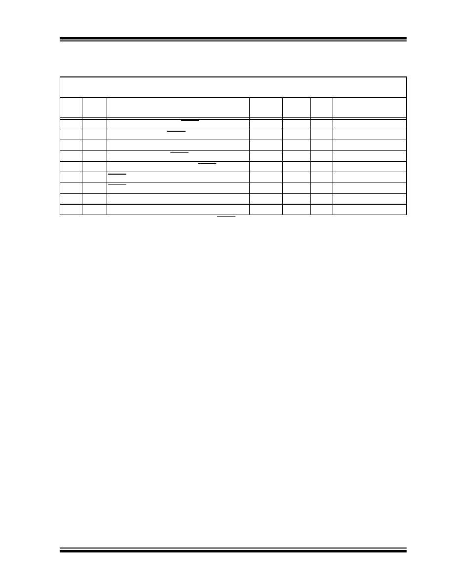
P12
THLD2
Input Data Hold Time from MCLR/VPP/RE3
↑
2—
μs
P13
TSET2VDD
↑ Setup Time to MCLR/VPP/RE3 ↑
100
—
ns
P14
TVALID
Data Out Valid from PGC
↑
10
—
ns
P15
TSET3PGM
↑ Setup Time to MCLR/VPP/RE3 ↑
2—
μs
P16
TDLY8
Delay between Last PGC
↓ and MCLR/VPP/RE3 ↓
0—
s
P17
THLD3MCLR/VPP/RE3
↓ to VDD ↓
—
100
ns
P18
THLD4MCLR/VPP/RE3
↓ to PGM ↓
0—
s
P19
THIZ
Delay from PGC
↑ to PGD High-Z
3
10
nS
P20
TPPDP
Hold time after VPP changes
5
—
μs
6.0
AC/DC CHARACTERISTICS TIMING REQUIREMENTS FOR PROGRAM/
VERIFY TEST MODE (CONTINUED)
Standard Operating Conditions
Operating Temperature: 25
°C is recommended
Param
No.
Sym.
Characteristic
Min.
Max.
Units
Conditions
Note 1:
Do not allow excess time when transitioning MCLR between VIL and VIHH; this can cause spurious program
executions to occur. The maximum transition time is:
1 TCY + TPWRT (if enabled) + 1024 TOSC (for LP, HS, HS/PLL and XT modes only) + 2 ms (for HS/PLL mode only)
+ 1.5
μs (for EC mode only) where TCY is the instruction cycle time, TPWRT is the Power-up Timer period and
TOSC is the oscillator period. For specific values, refer to the Electrical Characteristics section of the device data
sheet for the particular device.
发布紧急采购,3分钟左右您将得到回复。
相关PDF资料
PIC18F258T-I/SOG
IC MCU FLASH 16KX16 28SOIC
PIC18F2515T-I/SO
IC MCU FLASH 24KX16 28SOIC
PIC16LF1933-I/SP
IC PIC MCU FLASH 4K 28-DIP
PIC18F2515-E/SP
IC MCU FLASH 24KX16 28-DIP
PIC18F23K20-I/SP
IC PIC MCU FLASH 4KX16 28-DIP
PIC18F2515-E/SO
IC MCU FLASH 24KX16 28SOIC
PIC24F08KL401-I/MQ
IC MCU 16BIT 8KB FLASH 20-QFN
PIC16C55A-04/SP
IC MCU OTP 512X12 28DIP
相关代理商/技术参数
PIC18F24K20-I/SO
功能描述:8位微控制器 -MCU 16KB Flash 768B RAM 25 I/O 8B RoHS:否 制造商:Silicon Labs 核心:8051 处理器系列:C8051F39x 数据总线宽度:8 bit 最大时钟频率:50 MHz 程序存储器大小:16 KB 数据 RAM 大小:1 KB 片上 ADC:Yes 工作电源电压:1.8 V to 3.6 V 工作温度范围:- 40 C to + 105 C 封装 / 箱体:QFN-20 安装风格:SMD/SMT
PIC18F24K20-I/SP
功能描述:8位微控制器 -MCU 16KB Flash 768B RAM 25 I/O 8B RoHS:否 制造商:Silicon Labs 核心:8051 处理器系列:C8051F39x 数据总线宽度:8 bit 最大时钟频率:50 MHz 程序存储器大小:16 KB 数据 RAM 大小:1 KB 片上 ADC:Yes 工作电源电压:1.8 V to 3.6 V 工作温度范围:- 40 C to + 105 C 封装 / 箱体:QFN-20 安装风格:SMD/SMT
PIC18F24K20-I/SS
功能描述:8位微控制器 -MCU 16KB Flash 768B RAM 25 I/O 8B RoHS:否 制造商:Silicon Labs 核心:8051 处理器系列:C8051F39x 数据总线宽度:8 bit 最大时钟频率:50 MHz 程序存储器大小:16 KB 数据 RAM 大小:1 KB 片上 ADC:Yes 工作电源电压:1.8 V to 3.6 V 工作温度范围:- 40 C to + 105 C 封装 / 箱体:QFN-20 安装风格:SMD/SMT
PIC18F24K20T-I/ML
功能描述:8位微控制器 -MCU 16KB Flash 768B RAM 25 I/O 8B RoHS:否 制造商:Silicon Labs 核心:8051 处理器系列:C8051F39x 数据总线宽度:8 bit 最大时钟频率:50 MHz 程序存储器大小:16 KB 数据 RAM 大小:1 KB 片上 ADC:Yes 工作电源电压:1.8 V to 3.6 V 工作温度范围:- 40 C to + 105 C 封装 / 箱体:QFN-20 安装风格:SMD/SMT
PIC18F24K20T-I/SO
功能描述:8位微控制器 -MCU 16KB Flash 768B RAM 25 I/O 8B RoHS:否 制造商:Silicon Labs 核心:8051 处理器系列:C8051F39x 数据总线宽度:8 bit 最大时钟频率:50 MHz 程序存储器大小:16 KB 数据 RAM 大小:1 KB 片上 ADC:Yes 工作电源电压:1.8 V to 3.6 V 工作温度范围:- 40 C to + 105 C 封装 / 箱体:QFN-20 安装风格:SMD/SMT
PIC18F24K20T-I/SS
功能描述:8位微控制器 -MCU 16KB Flash 768B RAM 25 I/O 8B RoHS:否 制造商:Silicon Labs 核心:8051 处理器系列:C8051F39x 数据总线宽度:8 bit 最大时钟频率:50 MHz 程序存储器大小:16 KB 数据 RAM 大小:1 KB 片上 ADC:Yes 工作电源电压:1.8 V to 3.6 V 工作温度范围:- 40 C to + 105 C 封装 / 箱体:QFN-20 安装风格:SMD/SMT
PIC18F24K22-E/ML
功能描述:8位微控制器 -MCU 16KB Flash 768B RAM 8b FamilynanoWatt RoHS:否 制造商:Silicon Labs 核心:8051 处理器系列:C8051F39x 数据总线宽度:8 bit 最大时钟频率:50 MHz 程序存储器大小:16 KB 数据 RAM 大小:1 KB 片上 ADC:Yes 工作电源电压:1.8 V to 3.6 V 工作温度范围:- 40 C to + 105 C 封装 / 箱体:QFN-20 安装风格:SMD/SMT
PIC18F24K22-E/MV
功能描述:8位微控制器 -MCU 16KB Flash 768B RAM 8b FamilynanoWatt RoHS:否 制造商:Silicon Labs 核心:8051 处理器系列:C8051F39x 数据总线宽度:8 bit 最大时钟频率:50 MHz 程序存储器大小:16 KB 数据 RAM 大小:1 KB 片上 ADC:Yes 工作电源电压:1.8 V to 3.6 V 工作温度范围:- 40 C to + 105 C 封装 / 箱体:QFN-20 安装风格:SMD/SMT